Our core technologies
Below follows some short descriptions of our main research areas.
Active optical elements utilizing piezoMEMS
SINTEF is internationally recognized for its piezoMEMS technology which has led to start-ups such as poLight, Tunable and Sonair. You can read more about our piezoMEMS capabilities here.
Micromirrors
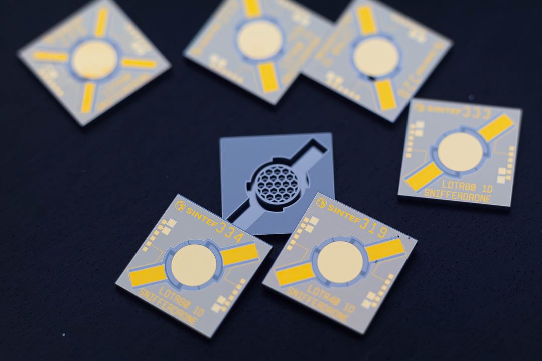
Utilizing our piezoMEMS capabilities allows us to provide a mature platform for long-stroke (10-100µm), low power (< 100 nW) and fast quasi-static (kHz) micromirrors for e.g. laser scanning, optical communication, IR-filtering, etc. In combination with our micro- and nanopatterning capabilities, the mirrors can be given advanced dielectric coatings or diffractive patterns. The mirror surfaces can be rigid planar surfaces or can be made to allow for focusing/defocusing through imposing curvature that can be modulated through ±160 diopters upon voltage application. Read our article on Small Mirrors, Major Advances.
Waveguides (PIC)
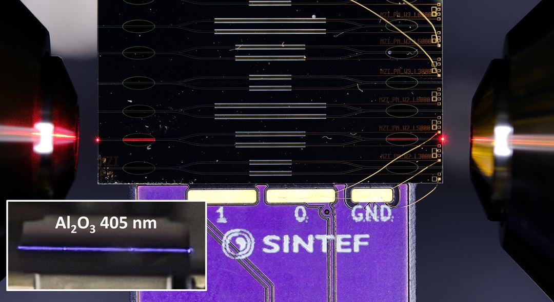
Integrating light into chips paves the way for miniaturizing optical sensing and novel low power computation. Our activities within photonic integrated circuits are:
- Active PIC: Using piezoelectric PZT we have made MEMS-actuated Mach-Zehnder Interferometers and utilized the electro-optic effect of PZT to realize plasmonic couplers.
- Waveguides beyond telecom wavelengths: Using novel materials Al2O3 and Al3N4 we can extend the transmission window from UV to NIR.
- Production services: We offer 6’’ wafer production services utilizing Si3N4 and Al2O3 material platforms.
Adaptive Metasurfaces
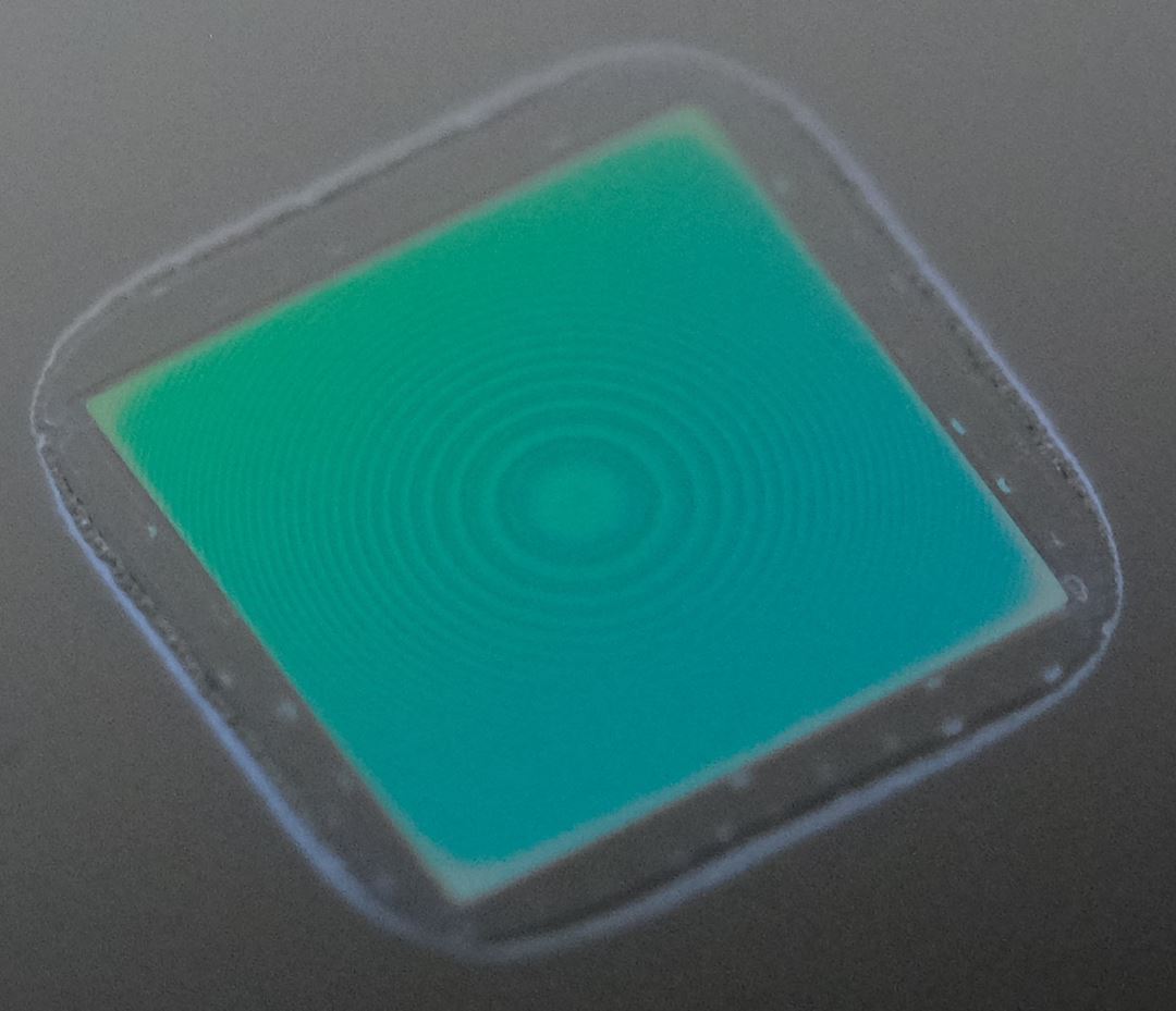
Arrays of intentionally designed sub-wavelength nanostructures opens for unprecedented control of light. We are for instance working to use MEMS actuated metasurfaces to detect tissue cancer by use of polarized light. We have made significant contributions to the research front in terms of:
- Non-hermitian elements: Science Advances 10.5 (2024): eadl4661
- Tunable waveplates: Nature communications 13.1 (2022): 2071.
- Varifocal lens: Optics Letters 47.5 (2022): 1049-1052
- Switchable meta-gratings: Science Advances 7.26 (2021): eabg5639
- Optimized metasurface fabrication processes for MEMS foundries: Nanomaterials 2023, 13(3), 436
Predefined SERS surfaces
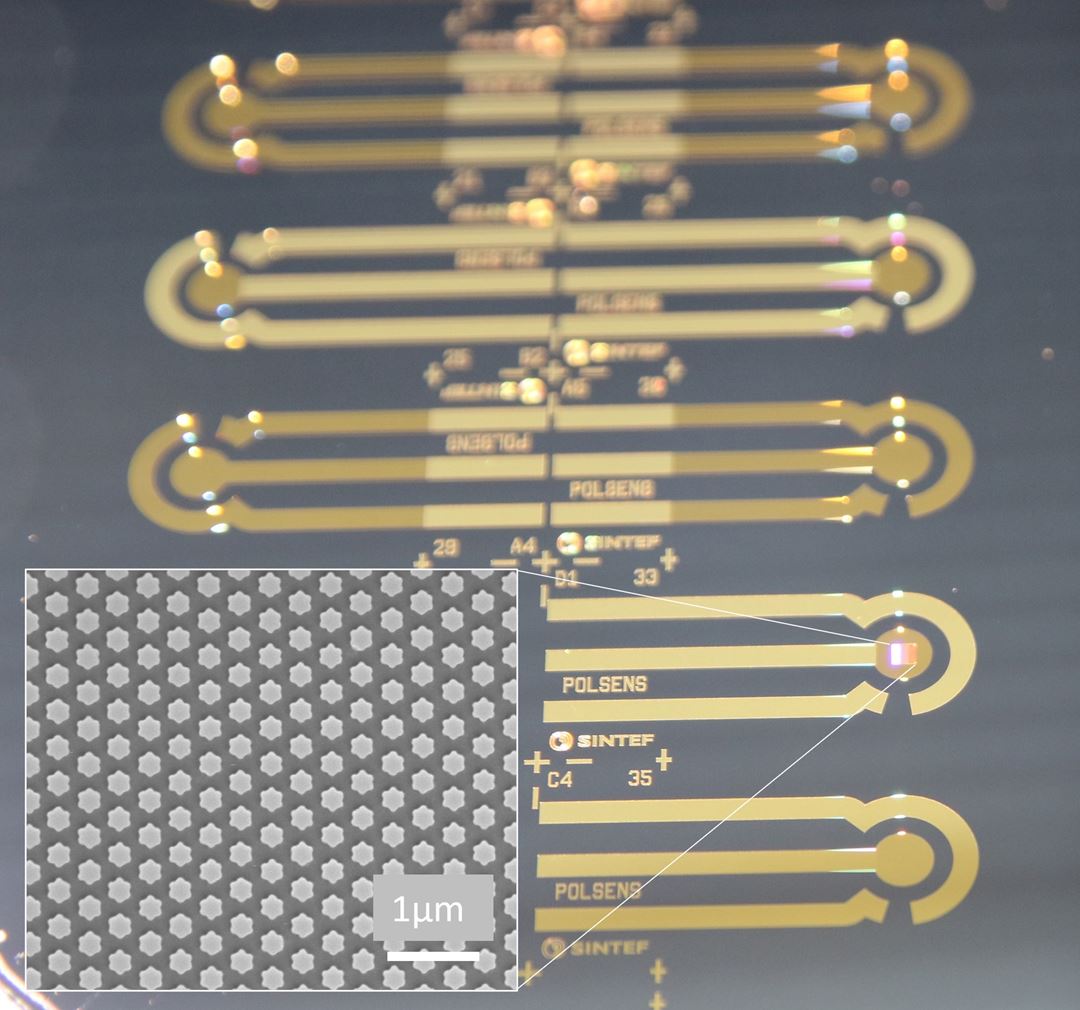
The design of SERS (Surface-Enhanced Raman Scattering) substrates directly influences the enhancement factor and sensitivity of the Raman signal. By optimizing the size, shape, and arrangement of nanostructures, we can create hotspots where the electromagnetic field is significantly intensified. This allows for the detection of even trace amounts of analytes, making SERS an incredibly powerful tool for chemical and biological sensing. Utilizing UV-Nanoimprint Lithography, we fabricate predefined SERS nanopatterns that are reproducible at low cost and high throughput. We are currently using these SERS substrates as a platform for monitoring water quality (read more about this here in Norwegian and here). In addition to water quality monitoring, our SERS substrates have potential applications in environmental sensing, medical diagnostics, and chemical detection.
IR sources
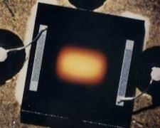
We have worked with silicon-based thermal IR-sources since the 70s-80s, and currently produce several variants for various industrial customers in gas sensing. Our research efforts have lately concentrated on dramatically reducing the energy consumption of such sources and making them directional.
Small scale production
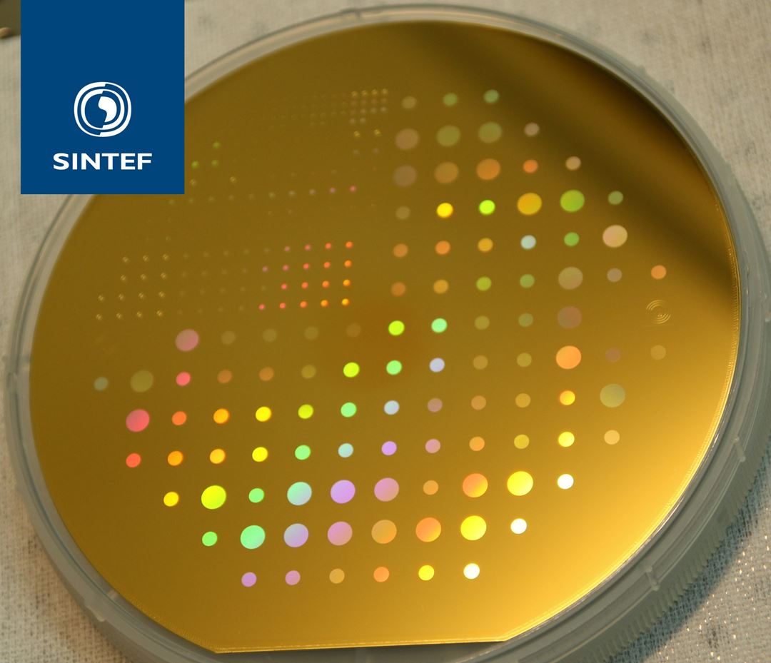
As the only complete, independent silicon chip research and fabrication line in Norway, SINTEF MiNaLab serves as a combined R&D&I and industrial small scale production pilot line. MiNaLab covers the full range from idea to manufacturing, supporting a “lab-to-fab” strategy. MiNaLab has established leading edge technology platforms and supplies devices to companies both in and outside Norway. Our cleanroom facility is industry focused, and we routinely complete production for new and established industry: We have e.g. delivered 300’000+ pressure sensors to the aviation industry and more than 180’000 radiation detectors for scientific instrument providers.
The SINTEF MiNaLab processing line is currently for 150 mm wafers with a focus on silicon sensors and actuators, including micro-optics and PICs, micro electromechanical systems (MEMS), silicon radiation detectors, as well as medical sensors and bioMEMS. MiNaLab’s pilot line operation is certified according to ISO 14001, ISO 9001 and ISO 45001.
Licensing opportunities
We have secured central IP rights to our technology portfolio. Contact us if you are interested in discussing licensing opportunities.
Contact
We exist for collaborative research and are continuously evaluating new application areas. Please feel free to contact us if you have an idea for collaboration you would like to discuss!

