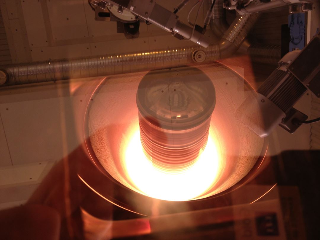
The research and development of crystal growth processes at SINTEF is driven by the demands which arises from this specific applications. Common goals are to improve the material properties at the micro and macroscale resulting in higher solar cell conversion efficiencies, increase of crystal dimensions and yield and, at the same time, a reduction of production costs and time.
Crystal growth from the melt is the most common process. It provides the basic silicon crystalline material for photovoltaic applications. The grown crystals are cut into wafers, which are further processed to solar cells and integrated into solar panels.
SINTEF works closely with the industry, but also operates an in-house crystallisation platform in conjunction with characterisation laboratories for testing and development of new products and processes.
Methods:
- Czochralski pulling of single crystals:
- Control of oxygen and crystal defects
- Increase productivity
- Testing of new raw materials
- Furnace design and optimization
- Training and technology transfer
Directional solidification of multi-crystalline silicon:
- Control of impurities
- Control of structure and defects for high efficient solar cells
- Testing and development of new furnace materials
- Testing of Si-feedstock
- Electromagnetic stirring
- Refining of Si using directional solidification

