 |
|
|
 |
|
Silicon/Glass Multi Project Wafer services
Low cost prototyping and limited volume production are possible with Multi Project Wafer (MPW) services in which devices of different customers are fabricated in a single wafer run. Since multiple customers share the same mask set, the costs of mask making and fabrication are divided.
MPW processing
The microBUILDER project provides access to state-of-the-art MEMS technologies at SensoNor Technologies and TRONICS Microsystems. The MPW processes are fully documented in the microBUILDER design handbook. Customers have the choice to either use the microBUILDER services for designing a device or to design their own component. For this purpose, special training courses are provided.
Features of the SensoNor Technologies MPW process
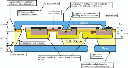
The MultiMEMS MPW process offers buried conductors and piezoresistors, thin silicon diaphragms, cantilevers and channels as well as glass and silicon cavities in a triple-stack anodic bonded configuration. Chip size 3 x 3 mm², 3 x 6 or 6 x 3 mm², or 6 x 6 mm²
Schematic outline of the Infineon SensoNor MPW process Schedule for the Infineon SensoNor MPW process
_____________________________________________________________________ Features of the TRONICS Microsystems process
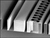
The TRONICS MPW process provides silicon channels, mixing pillars, heating electrodes and impedance sensing electrodes.
Schedule for the Tronics MPW process, running three times each year
Costs for the Tronics MPW run. For each location Tronincs deliver 20 chips
|
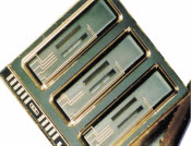
Silicon cleanroom facility Application examples prosessed by the SensoNor MPW service:
Micro balance, designed at SINTEF
Part of an electromagnetic-actuated microfluid pump, designed at CNM
Fluidic resonators, designed at CNM
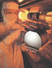
Clean-room fabrication facilities
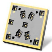
Application examples prosessed by Tronics: Capacitive structure
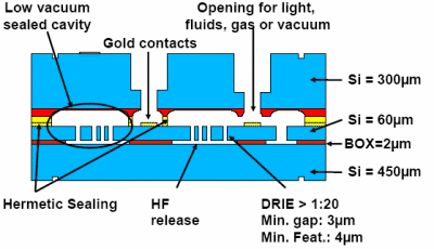
Wafer Level Vacuum Packaging concept | ||||||||||||||||||||||||||||||||||||||||||||||||||||||||||||||||